FPGA Prototyping and Design with the Lattice LFE2-12E-6FN256C LatticeECP2 Family FPGA
Field-Programmable Gate Arrays (FPGAs) have become indispensable in modern electronics, offering a flexible platform for prototyping, testing, and deploying digital logic designs. Among the diverse offerings in the market, the LatticeECP2 family stands out for its balance of performance, power efficiency, and cost-effectiveness. The Lattice LFE2-12E-6FN256C is a specific member of this family, providing a robust foundation for a wide range of applications, from consumer electronics to industrial control systems.
The LatticeECP2 series is built on a 90nm CMOS process, integrating a high-performance FPGA fabric with dedicated hard IP blocks. The "LFE2-12E" denotes a device with 12,000 LUTs (Look-Up Tables), which are the fundamental building blocks for implementing custom logic. The "-6" speed grade indicates a mid-range performance tier, suitable for many applications with moderate timing requirements. The package, "FN256C," is a 256-pin Fine-Pitch BGA (Ball Grid Array), which offers a compact footprint but requires careful PCB design and assembly processes.
A significant advantage of the LatticeECP2 family is its low-power operation. The architecture is optimized for power-sensitive applications, making it an excellent choice for portable and battery-powered devices. Furthermore, this FPGA features an embedded DSP (Digital Signal Processing) block, which can efficiently handle multiplication and accumulation operations, accelerating algorithms for signal filtering, audio processing, or image manipulation without consuming valuable general-purpose logic resources.
For connectivity, the device includes hardened IP for SERDES (Serializer/Deserializer) technology. This allows for the implementation of high-speed serial interfaces like PCI Express or Gigabit Ethernet directly on the FPGA, reducing the need for external PHY chips and simplifying board layout. The abundance of programmable I/Os supports various single-ended and differential I/O standards (LVCMOS, LVTTL, LVDS), providing the flexibility to interface with a wide array of other components, from sensors and memories to processors and display controllers.
The design workflow for this FPGA typically begins with hardware description languages (HDLs) like VHDL or Verilog. Designers describe the desired functionality through code, which is then synthesized into a netlist—a representation of the logic gates and their connections. The next critical phase is place-and-route (PAR), where the FPGA's proprietary software tools map the netlist onto the actual resources (LUTs, DSPs, I/Os) of the LFE2-12E device. This stage is crucial for meeting timing closure, ensuring that all signals propagate through the logic paths within one clock cycle. Lattice provides the ispLEVER Classic Design Suite (now superseded by Lattice Radiant) for this complete design flow, from synthesis and simulation to bitstream generation.
Finally, the configured design is loaded onto the FPGA via a JTAG interface, turning the generic hardware into a specialized computing engine. This capability for rapid prototyping is perhaps its greatest strength, allowing engineers to iterate on designs, test algorithms in real-time, and validate system integration long before committing to the expense of an ASIC (Application-Specific Integrated Circuit) tape-out.
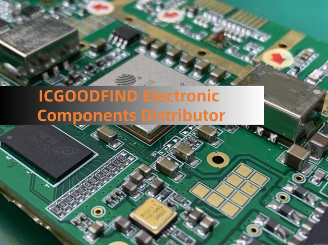
ICGOODFIND: The Lattice LFE2-12E-6FN256C FPGA provides a compelling blend of adequate logic capacity, integrated high-speed serial I/O, and low power consumption, making it a versatile and economical choice for engineers developing complex digital systems and bringing prototypes to life.
Keywords: FPGA Prototyping, LatticeECP2, Low-Power Design, Place-and-Route, SERDES

